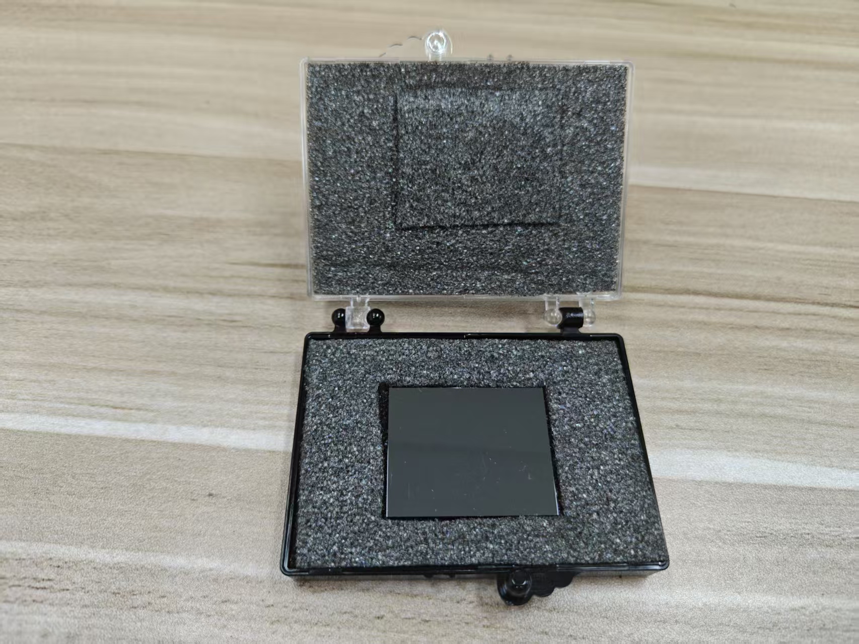
## Manifestation of Stacking Faults in the Electrical Behavior of CZT Crystals
Stacking faults in
Cadmium Zinc Telluride (CZT) crystals are planar crystallographic defects that result from interruptions or irregularities in the normal stacking sequence of atomic planes. These faults profoundly affect the electrical properties of CZT, especially in devices designed for radiation detection, where precise charge transport is critical for performance. The presence of stacking faults influences carrier mobility, trapping, recombination, and ultimately the detector signal quality.
## Nature and Formation of Stacking Faults in CZT
Stacking faults arise during crystal growth due to fluctuations in growth conditions, impurities, or lattice mismatches. They form as planar disruptions typically along close-packed planes, such as {111} planes in the zinc-blende lattice of CZT. These faults introduce localized regions where the crystal symmetry and periodicity are disturbed, creating electronic states within the bandgap.
The density, size, and distribution of stacking faults vary with growth techniques, doping, and post-growth processing. High stacking fault densities are often correlated with poorer crystal quality and degraded device performance.
## Impact on Charge Carrier Transport
Stacking faults act as scattering centers and charge trapping sites for free carriers (electrons and holes) moving through the crystal lattice. The local disruption of periodic potential at the fault plane causes perturbations in the electronic band structure, which can form localized energy states within the forbidden gap.
Carriers encountering stacking faults can be temporarily trapped or scattered, leading to a reduction in carrier mobility and lifetime. This trapping delays the charge collection process and increases the probability of recombination, reducing the overall charge collection efficiency of CZT detectors.
## Electrical Inhomogeneity and Localized Field Distortions
The presence of stacking faults leads to spatial variations in electrical properties, causing electrical inhomogeneity within the CZT crystal. These planar defects can locally modify the internal electric field distribution by introducing localized charge accumulations or dipole moments due to trapped charges at the fault interfaces.
Such localized field distortions cause non-uniform carrier drift velocities and uneven charge collection, manifesting as signal non-linearity and pulse shape variations in CZT detectors. This effect contributes to degraded energy resolution and increased noise.
## Influence on Leakage Current and Noise
Stacking faults may contribute to increased leakage currents in CZT devices by introducing mid-gap states that facilitate thermally activated charge carrier generation. These defect states can act as generation-recombination centers, increasing the dark current under reverse bias conditions.
Elevated leakage currents contribute to higher electronic noise levels, deteriorating the signal-to-noise ratio of the detector and limiting its sensitivity.
## Effects on Charge Trapping and Polarization
Charge trapping at stacking faults exacerbates polarization effects commonly observed in CZT detectors. Trapped charges accumulate over time, creating internal fields that oppose the applied bias voltage, reducing effective carrier drift and collection efficiency.
This phenomenon leads to temporal degradation of detector response, commonly referred to as polarization, which adversely impacts long-term stability and measurement accuracy.
## Detection and Characterization via Electrical Measurements
The electrical manifestations of stacking faults are often observed indirectly through techniques such as current-voltage (I-V) characterization, transient current techniques, and pulse shape analysis. Deviations from ideal charge transport behavior, such as increased trapping times, lower carrier mobility-lifetime products, and anomalous leakage currents, can indicate the presence of stacking faults.
Combined with structural characterization methods like transmission electron microscopy (TEM), electrical measurements help correlate stacking fault density with device performance metrics.
## Mitigation and Control Strategies
Minimizing stacking faults during CZT crystal growth is vital for enhancing electrical performance. Techniques include optimizing growth parameters (temperature gradients, growth rates), using seed crystals with low defect densities, and carefully controlling doping concentrations.
Post-growth treatments, such as annealing, may reduce stacking fault density or mitigate their electrical impact by enabling defect recombination or passivation.
## Summary
Stacking faults in CZT crystals manifest electrically by introducing localized trapping centers, scattering sites, and mid-gap states that degrade carrier mobility, increase leakage currents, distort internal electric fields, and induce polarization effects. These consequences reduce charge collection efficiency, increase noise, and impair energy resolution in CZT-based detectors. Understanding and controlling stacking fault formation is critical for optimizing the electrical behavior and reliability of CZT crystal devices in radiation detection applications.
CdZnTe Association (CdZnTe.com)
https://www.cdznte.com/blog/how-do-stacking-faults-manifest-in-the-electrical-behavior-of-czt-crystal.html