## Influence of Contact Geometry on Electric Field Shaping in CZT Crystal Devices
Contact geometry plays a crucial role in determining the spatial distribution of the electric field within
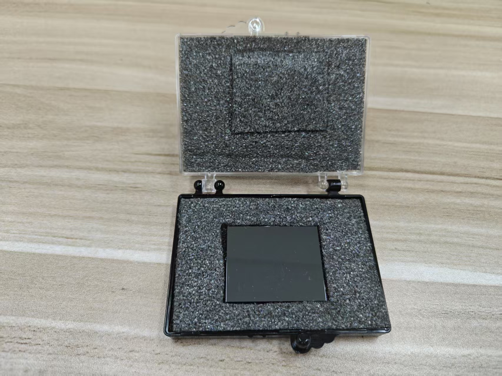
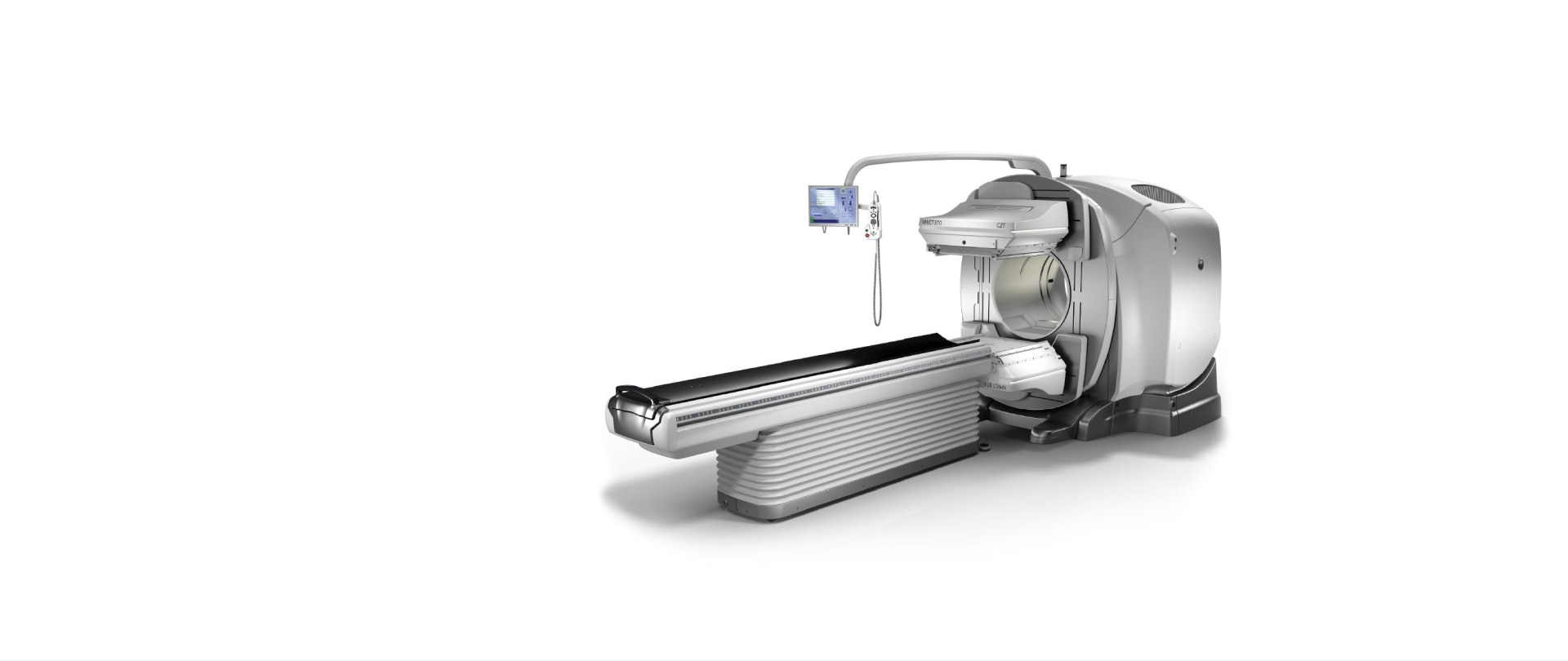
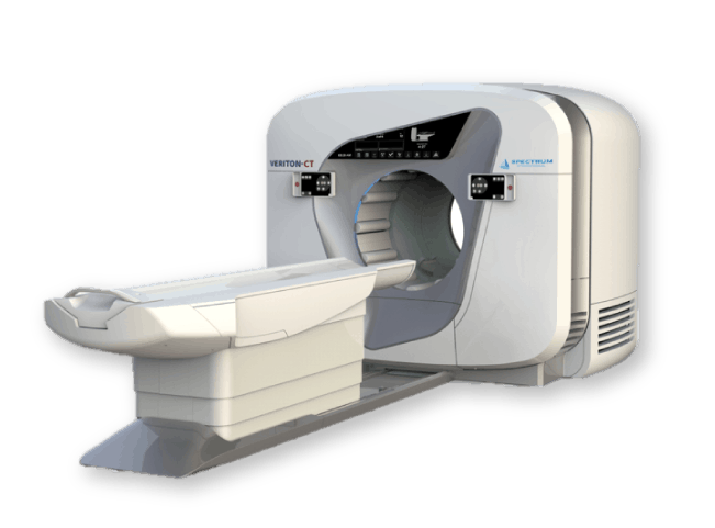
Cadmium Zinc Telluride (CZT) crystal devices. Since CZT crystals are widely used in radiation detectors, such as gamma-ray spectrometers, shaping the electric field effectively inside the bulk material is essential to optimize charge collection efficiency, reduce trapping effects, and enhance energy resolution. The contact design directly affects the internal electric field profile, which governs the drift paths and velocities of charge carriers generated by radiation interactions.
## Fundamental Role of Contacts in Electric Field Formation
The metal-semiconductor contacts on CZT crystals define the boundary conditions for the internal electric field. When a bias voltage is applied across the contacts, an electric field is established inside the crystal that drives the motion of electrons and holes toward the respective electrodes. The shape, size, spacing, and arrangement of these contacts influence how this field distributes throughout the crystal volume.
A uniform and well-shaped electric field is desired for optimal charge transport and minimal charge trapping, which improves the detector’s signal fidelity. However, imperfect or non-ideal contact geometries can lead to field distortions, non-uniform carrier drift velocities, and increased recombination or trapping at defect sites.
## Effect of Contact Size and Shape
The size and shape of the contacts critically affect local electric field intensities near the contact surfaces. For example, large-area planar contacts tend to produce relatively uniform fields in the bulk but can also lead to high-field regions near the edges due to field fringing effects.
Smaller or segmented contacts, such as pixelated or strip geometries, introduce localized field variations. In pixelated detectors, each pixel electrode acts as a small anode with a unique field distribution around it. This localized field shaping improves spatial resolution by confining charge collection to smaller volumes but also increases complexity in field uniformity. The field lines tend to concentrate near the pixel edges, potentially leading to enhanced carrier trapping or surface recombination in these regions.
Contact shapes with rounded edges or specially engineered guard rings can reduce field crowding and minimize high-field regions that might cause premature breakdown or increased noise. Sharp corners in contact geometry often create electric field hotspots, which can accelerate degradation or increase leakage currents.
## Impact of Contact Spacing and Arrangement
The spacing between contacts, especially in multi-electrode configurations like pixel arrays or strip detectors, strongly affects the electric field distribution. Narrow gaps between contacts result in strong lateral fields, which can help steer charge carriers more efficiently toward the collecting electrodes but may also cause field non-uniformities and cross-talk between adjacent pixels.
Wider spacing tends to produce more uniform fields within each pixel volume but may reduce spatial resolution. Optimizing contact pitch is therefore a balance between electric field uniformity, spatial resolution, and charge collection efficiency.
Moreover, the arrangement of contacts (e.g., coplanar grids, pixel arrays, or Frisch grids) modifies the electric field topology inside the CZT crystal. For instance, coplanar grid detectors employ interleaved electrodes to shape the field selectively and to mitigate the effects of poor hole transport by weighting the electron signal more heavily, resulting in improved energy resolution.
## Influence on Charge Carrier Drift and Trapping
Electric field shaping by contact geometry determines the drift trajectories of electrons and holes generated by ionizing radiation within the CZT crystal. Well-designed contact geometries create uniform fields that promote efficient carrier transport with minimal trapping and recombination.
Non-uniform fields caused by suboptimal contact geometry can induce regions of low or zero field (“dead zones”) where carriers move slowly or are trapped. This results in incomplete charge collection and degrades the detector’s energy resolution.
Additionally, field gradients near the contacts influence carrier velocity. High-field regions accelerate carriers, reducing their transit time and probability of trapping, but excessive field concentrations can increase noise or cause breakdown.
## Guard Rings and Passivation Structures
Guard rings are auxiliary contacts placed around the primary electrodes to shape the electric field near the edges of the crystal. Their presence reduces surface leakage currents and mitigates edge effects by smoothing potential gradients. Guard rings influence the overall field distribution by preventing the formation of strong field crowding at device edges, thus improving detector stability and lifetime.
Passivation layers combined with carefully designed guard rings also help maintain surface charge neutrality, which affects the field shape near the crystal surface and prevents unwanted surface conduction paths that distort the internal electric field.
## Simulation and Modeling of Contact Geometry Effects
Finite element modeling (FEM) and other numerical techniques are extensively used to simulate how different contact geometries influence the electric field inside CZT devices. These simulations allow optimization of electrode shapes, sizes, and arrangements before fabrication, reducing trial and error.
Models show that subtle changes in contact geometry can significantly alter the internal field profiles, charge collection efficiency, and ultimately detector performance. Simulation results often guide the design of pixel sizes, guard ring dimensions, and biasing schemes to achieve the best compromise between energy resolution, spatial resolution, and operational stability.
## Summary
Contact geometry in CZT crystal devices critically influences electric field shaping, which directly impacts carrier transport, charge collection efficiency, and device performance. Key factors include the size, shape, and spacing of contacts, as well as the presence of guard rings and passivation layers. Properly engineered contact geometries produce uniform fields that enhance carrier drift, reduce trapping, and improve detector resolution, while poor geometries can cause field distortions, increased noise, and device degradation. Numerical modeling and simulations are essential tools for optimizing contact designs to achieve superior CZT detector performance.
CdZnTe Association (CdZnTe.com)
https://www.cdznte.com/blog/how-does-contact-geometry-affect-electric-field-shaping-in-czt-crystal-devices.html