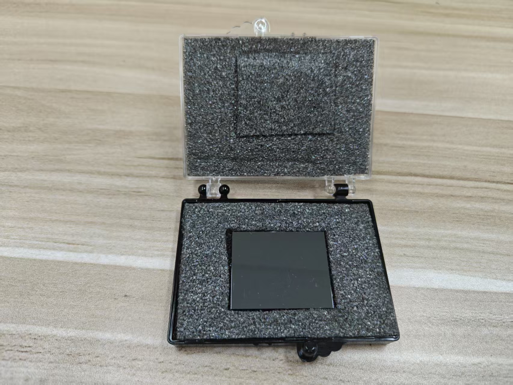
## Electric Field Distribution Within a Biased CZT Crystal Detector
The electric field distribution inside a biased
Cadmium Zinc Telluride (CZT) crystal detector plays a fundamental role in its performance, particularly affecting charge carrier transport, charge collection efficiency, and energy resolution. The electric field is established by applying a voltage bias across the electrodes of the detector, which drives the motion of charge carriers generated by radiation interactions within the crystal.
## Ideal Uniform Electric Field Assumption
In an ideal scenario, the electric field in a planar CZT detector with uniform electrodes is assumed to be
uniform and constant throughout the bulk of the crystal. This means the electric field lines are parallel and the field strength (magnitude) is consistent from the cathode to the anode. For a crystal of thickness $d$ biased by voltage $V$, the ideal electric field $E$ would be:
$$
E = frac{V}{d}
$$
Such a uniform field ensures consistent drift velocities for electrons and holes, enabling efficient charge collection and minimal charge trapping or recombination.
## Realistic Non-Uniform Electric Field Distribution
However, real CZT detectors often exhibit
non-uniform electric field distributions due to various factors including:
* Crystal imperfections and defects
* Space charge effects from trapped carriers
* Electrode geometry and contact properties
* Polarization effects under prolonged biasing
These factors cause deviations from the ideal uniform field, leading to spatial variations in electric field strength.
## Influence of Space Charge and Trapping
One of the most significant causes of electric field non-uniformity in CZT detectors is the presence of
space charge formed by trapped charge carriers. Traps within the CZT crystal capture free carriers, creating localized regions of net charge. This trapped charge modifies the local electric potential and thus distorts the electric field.
* Near the cathode, where electrons are generated and begin drifting toward the anode, trapped electrons can accumulate, forming a negative space charge region.
* Near the anode, trapped holes can form positive space charge regions.
This redistribution of charge alters the initially applied field, typically causing
field weakening or
field distortion in the central region of the crystal and field enhancement near the electrodes. The consequence is often a
field gradient rather than a constant field.
## Polarization Effect
Under prolonged bias and radiation exposure, the accumulation of trapped charges inside the CZT crystal can lead to
polarization, a phenomenon where the internal electric field is significantly distorted. Polarization manifests as a reduction of the electric field strength in the bulk and sometimes field inversion near the electrodes, reducing the detector’s charge collection efficiency and increasing noise.
Polarization often leads to:
* Decreased drift velocity in the bulk
* Increased carrier trapping and recombination
* Non-linear electric field profiles that can degrade spectral performance
## Effect of Electrode Geometry
The geometry and design of electrodes significantly influence the electric field distribution:
*
Planar Electrodes: In a simple planar electrode configuration, the field tends to be more uniform, but still can be distorted by space charge and traps.
*
Pixelated or Coplanar Grid Electrodes: Advanced electrode designs like coplanar grids create spatially varying fields designed to improve electron collection and reduce the influence of holes. These structures generate localized high-field regions near the collecting electrodes and lower field regions elsewhere, improving charge collection and signal resolution.
*
Guard Rings: Additional guard rings or shaping electrodes can be used to control surface fields and reduce leakage currents, helping to shape the overall field distribution near crystal edges.
## Depth-Dependent Electric Field Profiles
Measurements and simulations often show that the electric field strength in a biased CZT detector is not constant along the depth:
* The electric field may be stronger near the cathode or anode depending on trap distributions.
* A field minimum can appear in the middle of the crystal, leading to a "double-humped" or non-monotonic field profile.
* This variation affects carrier drift times, increasing the probability of trapping and recombination in regions of low field.
## Temperature Dependence
The electric field distribution can also be affected by temperature:
* At higher temperatures, increased carrier detrapping can partially neutralize space charge, leading to a more uniform field.
* Conversely, at low temperatures, traps can hold carriers longer, enhancing space charge effects and increasing field distortion.
## Summary
The electric field distribution in a biased CZT crystal detector is ideally uniform but often becomes non-uniform in practice due to space charge buildup, trap-related charge accumulation, electrode geometry, and polarization effects. These non-uniformities cause spatial variations in electric field strength, impacting carrier drift velocity, charge collection efficiency, and ultimately the detector’s energy resolution and performance. Optimizing electrode design and controlling material quality are critical strategies to minimize electric field distortion and enhance detector operation.
CdZnTe Association (CdZnTe.com)
https://www.cdznte.com/blog/how-does-electric-field-distribution-vary-within-a-biased-czt-crystal-detector.html