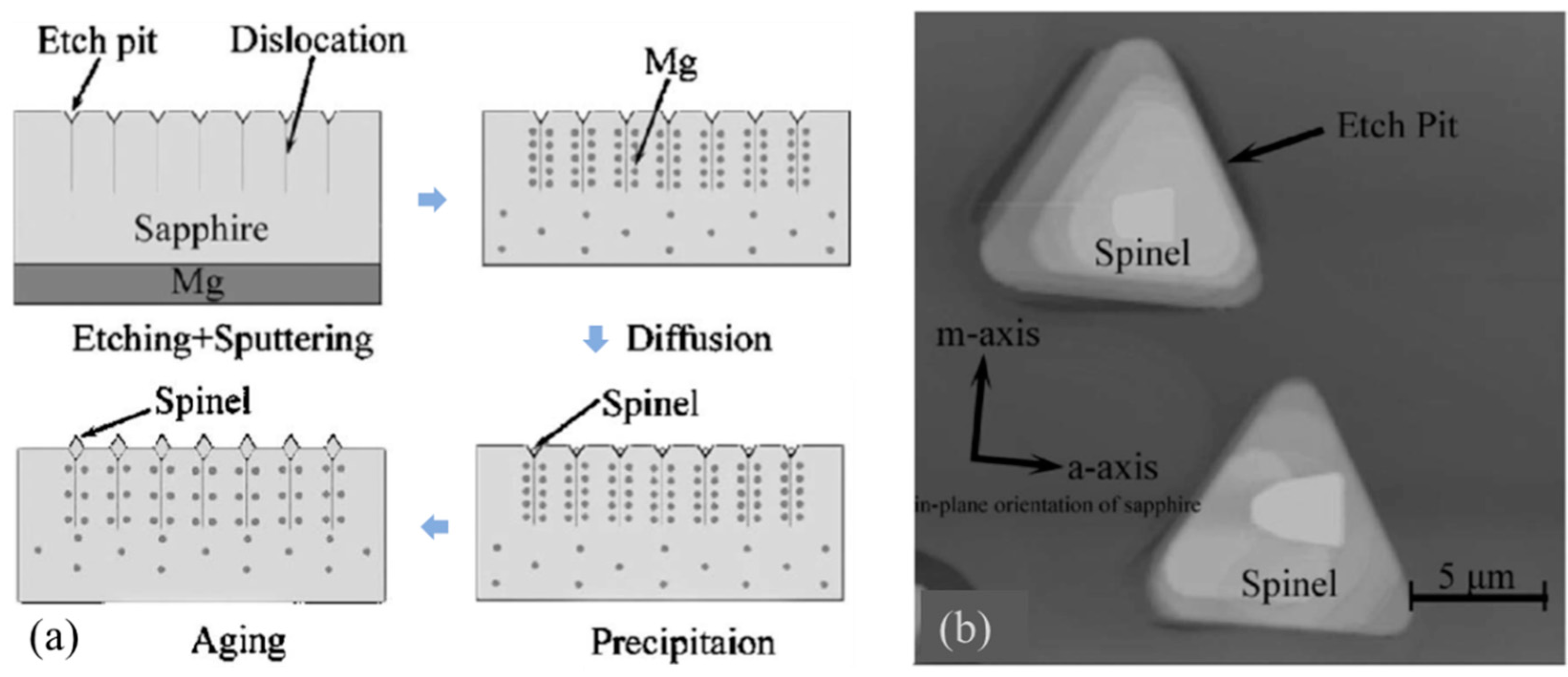
Etch pit density (EPD) measurement is a widely used, effective technique to assess the
crystalline quality and
defect density in CdZnTe (CZT) films, especially after thermal treatments such as annealing. It provides a direct and quantitative evaluation of
dislocation density and related structural imperfections in the crystal lattice, which are critical to device performance.
## Principle of Etch Pit Density Measurement
EPD involves chemically etching the CZT film surface with a selective etchant that preferentially attacks
defect sites such as
dislocations and
grain boundaries. These defects act as
etch initiation points, producing microscopic pits—called etch pits—visible under optical or electron microscopy. Counting the number of these pits per unit area yields the etch pit density, which correlates with the density of crystalline defects.
## Reflection of Changes in Crystalline Quality and Defect Density After Annealing
## 1. Reduction of Etch Pit Density Indicates Improved Crystalline Quality
* Annealing typically enhances atomic mobility, enabling
dislocations to rearrange, glide, or annihilate, and enabling point defects to migrate and recombine.
* As a result, the density of extended defects such as dislocations decreases, which manifests as a
lower etch pit density after annealing.
* A reduced EPD directly indicates
fewer dislocations, implying a
higher crystalline quality with less strain and fewer non-radiative recombination centers.
## 2. Correlation with Structural Relaxation and Defect Passivation
* The lowering of EPD after annealing often correlates with
lattice relaxation and
strain relief, as annealing can reduce lattice mismatch effects and defect accumulation near interfaces.
* Additionally, some point defects that act as etch initiation sites may be passivated or eliminated during annealing, further contributing to decreased etch pit formation.
* Thus, EPD reflects not only dislocation density but also the overall
defect landscape improvement.
## 3. Spatial Distribution and Uniformity
* EPD mapping across the wafer surface after annealing can reveal
non-uniformities in defect reduction.
* Areas with significantly lowered EPD correspond to regions of better crystalline quality and fewer structural defects.
* This spatial information helps optimize annealing parameters and assess film uniformity.
## 4. Limitations and Complementary Role
* While EPD is excellent for revealing
dislocation density, it is less sensitive to certain
point defects that do not form etch pits.
* Therefore, EPD should be used alongside other characterization techniques (e.g., photoluminescence, X-ray diffraction) for a comprehensive picture of crystalline quality and defect reduction.
## Summary
In annealed CdZnTe films,
etch pit density measurement is a sensitive indicator of changes in crystalline quality and defect density. A decrease in EPD after annealing clearly signifies a reduction in dislocation density and associated structural defects, reflecting enhanced crystal perfection, improved lattice relaxation, and defect passivation. This improvement is critical for optimizing CZT film properties for high-performance optoelectronic and radiation detector applications.
CdZnTe Association (CdZnTe.com)
https://www.cdznte.com/blog/how-does-the-etch-pit-density-measurement-reflect-changes-in-crystalline-quality-and-defect-density-in-annealed-cdznte-films.html



