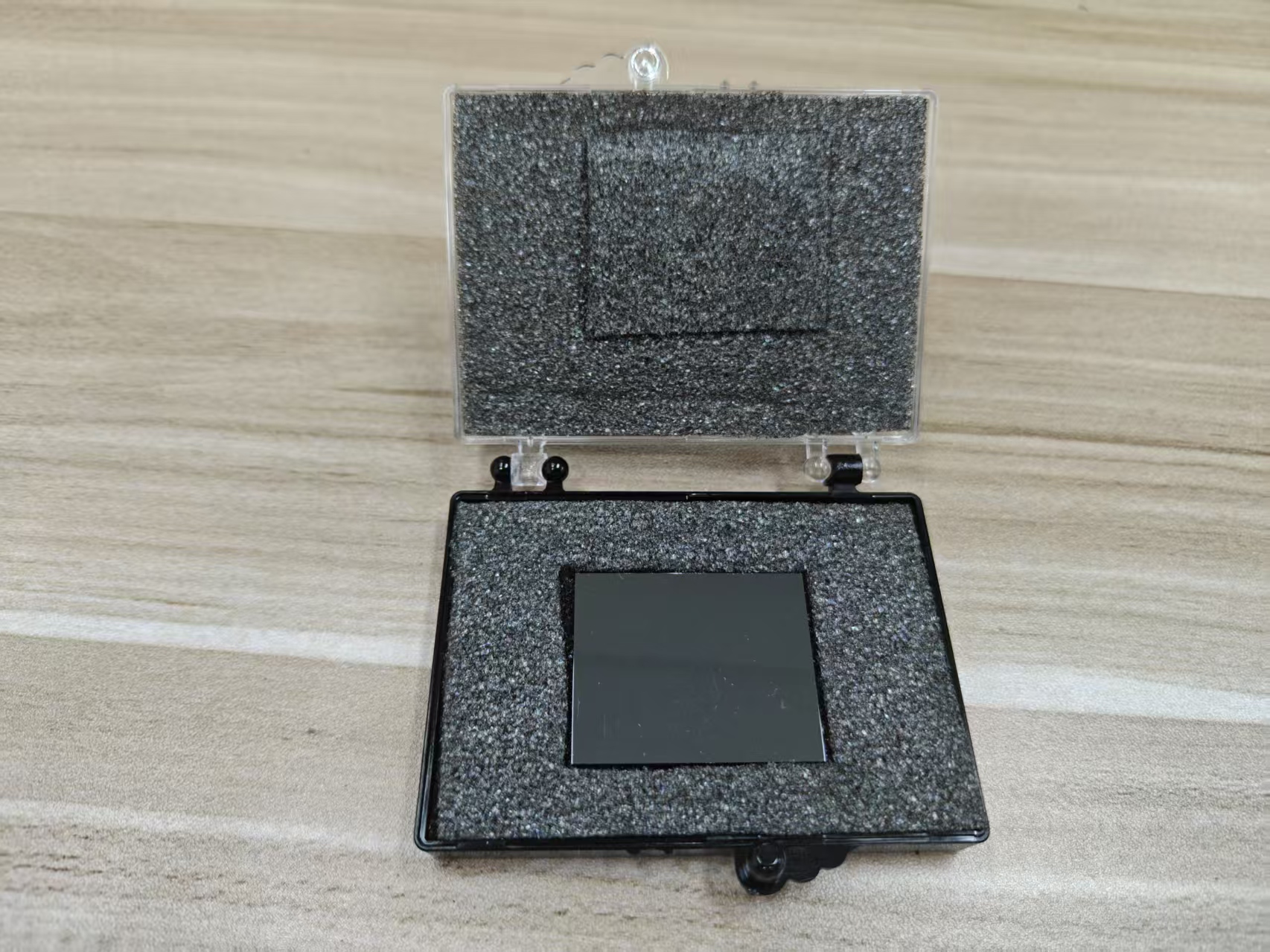
The manufacturing process of
Cadmium Zinc Telluride (CZT) detectors plays a significant role in determining the uniformity of the material, which in turn affects its performance in radiation detection applications. The uniformity of a CZT detector is crucial for ensuring consistent charge collection, energy resolution, and overall detection efficiency across the entire detector volume. Several factors in the manufacturing process—ranging from crystal growth to post-processing—can influence the uniformity of the CZT material. Below is a detailed explanation of how the various steps in the manufacturing process affect the uniformity of CZT detectors.
## 1. Crystal Growth Techniques
The first and most critical step in the manufacturing process that impacts the uniformity of CZT detectors is the crystal growth process. The quality of the crystal directly determines the uniformity of its properties, including composition, structural integrity, and defect distribution.
*
Bridgman Method: The vertical Bridgman technique is one of the most commonly used methods for growing CZT crystals. In this method, a charged ampoule containing cadmium, zinc, and tellurium is slowly cooled, leading to crystal formation. The cooling rate and temperature gradient during the process are crucial for ensuring uniform crystal growth. If the temperature is not carefully controlled, the crystal may develop imperfections such as phase separation or non-uniformity in the Cd:Zn ratio. This can lead to areas within the crystal with differing electrical properties, which can negatively affect the detector's performance.
*
High Pressure and High Temperature (HPHT) Growth: Another method is the HPHT technique, where the crystal is grown under elevated pressure and temperature conditions. This process typically allows for larger and more uniform crystals but requires precise control of the temperature and pressure throughout the growth process. Variations in pressure or temperature can lead to heterogeneity in the crystal's structure, including the presence of dislocations, grain boundaries, or other defects that can affect charge transport and collection efficiency.
*
Czochralski Process: This method, typically used for growing other semiconductor crystals, is less common for CZT but has been explored in certain applications. In the Czochralski method, a seed crystal is dipped into a melt and slowly pulled upwards while rotating, leading to a single crystal formation. While this method can produce high-quality crystals, it may also introduce structural inhomogeneities if the melt is not uniformly maintained or if the pull rate is too fast.
*
Temperature Gradient: A non-uniform temperature gradient during the cooling process can result in a variation in the crystal structure, which leads to uneven electrical properties. In the Bridgman method, the cooling rate must be carefully controlled to ensure that the crystal solidifies uniformly. A rapid cooling rate can cause thermal stresses or inhomogeneities, while a slow rate may allow unwanted defects to form.
## 2. Material Purity and Homogeneity
The purity of the raw materials and the homogeneity of the mixture are crucial in the manufacturing process. Impurities and uneven distributions of the elements (cadmium, zinc, and tellurium) can result in localized areas of higher or lower conductivity, charge trapping, and poor charge collection efficiency.
*
Purity of Raw Materials: If the raw materials (cadmium, zinc, tellurium) are not pure, impurities can introduce additional defect states or charge carrier traps in the CZT crystal. These impurities may lead to a non-uniform distribution of electrical properties across the detector material. For example, trace amounts of iron or copper can act as deep-level traps, reducing the overall performance of the CZT detector and causing non-uniformity in the charge collection efficiency.
*
Homogeneity of the Melt: Achieving a homogeneous mixture of cadmium, zinc, and tellurium in the molten state is essential for producing a uniform CZT crystal. If the components are not uniformly mixed, the resulting crystal may have regions with different Cd:Zn ratios or defect densities, leading to inhomogeneous electrical behavior. A uniform melt composition ensures that the crystal structure grows consistently throughout the entire ingot.
## 3. Crystal Cutting and Shaping
Once the CZT crystal is grown, it must be cut and shaped into the desired form for detector applications. This step can introduce additional challenges in maintaining uniformity.
*
Crystal Orientation and Grain Boundaries: During the cutting process, it is important to maintain proper crystal orientation. Cutting across grain boundaries or misaligned crystal planes can lead to regions of higher resistance or charge trapping, affecting the detector's overall performance. Proper orientation also helps minimize the risk of electrical shorts or non-uniform response across the crystal.
*
Inhomogeneity Due to Cracking: Mechanical stress during cutting and shaping can cause the CZT crystal to crack, leading to structural inhomogeneity. Cracks and micro-defects introduced during the cutting process can act as trapping centers for charge carriers, which affect the uniformity of charge collection and result in reduced performance.
## 4. Electrode Deposition
After the CZT crystal is cut into the desired shape, electrodes must be deposited on the crystal to collect charge carriers. The deposition process plays a crucial role in ensuring uniformity in the detector's performance.
*
Electrode Material and Thickness: The choice of electrode material (e.g., gold, nickel, or copper) and the uniformity of its deposition can influence the performance of the CZT detector. Non-uniform electrode deposition can create localized variations in the electric field, which can lead to uneven charge collection. Additionally, thin or poorly deposited electrodes may introduce contact resistance, which can further affect uniformity.
*
Electrode Geometry and Distribution: The geometry and distribution of the electrodes also affect the uniformity of charge collection. For example, a non-uniform electrode design or poorly placed contacts may result in uneven electric fields, causing charge carriers to be unevenly collected across the detector. Using
field-shaping electrodes or multi-electrode arrays can help improve uniformity by ensuring that the electric field is distributed more uniformly across the entire crystal.
## 5. Post-Growth Treatment and Annealing
Post-growth treatments such as annealing can significantly affect the uniformity of the CZT detector. Annealing is used to modify the crystal structure, reduce defects, and improve charge transport properties. However, if not carefully controlled, annealing can lead to non-uniform changes in the material.
*
Annealing Temperature and Time: The annealing process involves heating the CZT crystal to a high temperature and then gradually cooling it. If the temperature or cooling rate is not uniform, certain regions of the crystal may undergo different changes in defect density, leading to inhomogeneity. For instance, excessive or uneven heating during annealing may result in the formation of new defect sites or the migration of existing defects, which can affect the uniformity of the charge collection efficiency.
*
Effect of Annealing on Defects: While annealing can help reduce defects such as dislocations or vacancies, improper annealing may exacerbate these defects or introduce new types of traps that cause non-uniformities. Additionally, thermal gradients during annealing can lead to residual stresses, which may manifest as cracks or uneven distributions of electrical properties.
## 6. Doping and Compensation
In some cases, dopants are added to the CZT material to improve certain properties, such as charge carrier concentration or the suppression of charge trapping. The doping process must be carefully controlled to maintain uniformity.
*
Doping Uniformity: Non-uniform doping can lead to regions of the CZT detector with differing electrical properties, such as varying resistivity or carrier concentration. This can result in localized variations in charge collection efficiency, which can degrade the detector's performance. Dopants must be introduced in a controlled manner to ensure a homogeneous distribution throughout the crystal.
*
Compensation for Deep-Level Traps: In certain cases, compensation methods such as introducing p-type or n-type dopants can help reduce the effects of deep-level traps. However, improper compensation can lead to regions with excessive doping, leading to non-uniform behavior in the detector.
## 7. Surface Processing and Passivation
The final step in the manufacturing process involves surface treatment and passivation. The surface quality of the CZT crystal can affect the uniformity of charge collection, as surface defects can act as recombination centers for charge carriers.
*
Surface Polishing: The surface of the CZT crystal must be carefully polished to remove any mechanical imperfections or surface defects. Uneven polishing or surface roughness can create regions with higher recombination rates, affecting charge collection uniformity. Additionally, any residual stresses induced during polishing can lead to localized performance variations.
*
Passivation Layers: Applying a passivation layer helps reduce surface recombination by creating a protective barrier that prevents charge carriers from being trapped at the surface. The uniformity of this passivation layer is crucial to ensure that no areas of the detector are more prone to charge loss than others. Non-uniform passivation can lead to inhomogeneous detector performance.
## Conclusion
The manufacturing process has a profound impact on the uniformity of CZT detectors. Variations in crystal growth, material purity, electrode deposition, post-growth treatments, doping, and surface processing can all contribute to non-uniformities that affect the detector's performance. A carefully controlled manufacturing process is required to minimize these effects and ensure that the CZT crystal maintains consistent properties across the entire detector. This uniformity is essential for achieving high energy resolution, efficient charge collection, and reliable performance in radiation detection applications. Therefore, optimizing each step of the manufacturing process is crucial for producing high-quality, uniform CZT detectors.
CdZnTe Association (CdZnTe.com)
https://www.cdznte.com/blog/how-does-the-manufacturing-process-affect-the-uniformity-of-czt-detectors.html