## Introduction
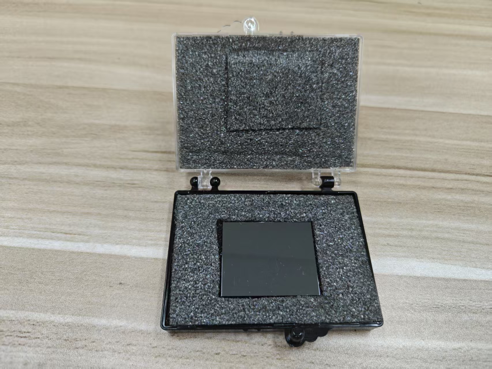
The small pixel effect is a crucial phenomenon exploited in CdZnTe (
Cadmium Zinc Telluride) radiation detectors to mitigate the inherent issue of poor hole transport and collection inefficiency. CdZnTe detectors are favored for room-temperature gamma-ray and X-ray detection due to their wide bandgap and high atomic number. However, the intrinsic material properties of CdZnTe, such as the significantly lower mobility-lifetime product (μτ) for holes compared to electrons, lead to hole trapping and incomplete charge collection. The small pixel effect leverages electrode geometry to suppress the influence of holes on the induced signal, thereby improving energy resolution and charge collection performance.
## Hole Collection Inefficiency in CdZnTe Detectors
Hole collection inefficiency arises primarily from the disparity between electron and hole transport properties in CdZnTe. Electrons generally have higher mobility and longer lifetime (higher μτ), enabling efficient drift and collection at the anode. Conversely, holes exhibit lower mobility and shorter lifetime, causing them to be trapped or recombine before reaching the cathode. This trapping leads to incomplete charge collection, signal distortion, low-energy tailing in spectra, and degraded energy resolution.
Hole trapping also results in position-dependent signal variation because the fraction of the total charge induced by holes depends on the carrier transit path length. Reducing the contribution of holes to the total induced charge signal is therefore essential to improving detector performance.
## Principle of the Small Pixel Effect
The small pixel effect originates from the spatial dependence of the weighting potential in pixelated detectors. Weighting potential is a conceptual electrostatic potential that describes how the movement of charge carriers induces signal current on a given electrode according to the Shockley-Ramo theorem.
*
Localized Weighting Potential: In detectors with very small pixel electrodes compared to the detector thickness, the weighting potential is highly localized near each pixel. It rises sharply only very close to the pixel electrode and remains near zero elsewhere in the bulk.
*
Electron Signal Dominance: Since electrons drift toward the anode pixels, they traverse regions of increasing weighting potential and thus induce strong charge signals. Holes, however, drift toward the cathode on the opposite side, in regions where the weighting potential relative to the pixel electrode remains near zero or very low, inducing minimal signal despite their physical movement.
*
Reduced Hole Contribution: Because the weighting potential associated with holes is small due to their path being largely outside the pixel's localized weighting potential, the holes’ contribution to the total induced charge on the small pixel electrode is significantly suppressed. This effectively reduces the impact of hole trapping on the measured signal.
## How the Small Pixel Effect Improves Hole Collection Inefficiency
*
Mitigation of Hole Trapping Effects: By reducing the hole-induced component of the charge signal, the small pixel effect minimizes the signal degradation caused by hole trapping. The measured charge signal becomes dominated by electrons, which are less prone to trapping, thereby improving energy resolution.
*
Reduction of Low-Energy Tail: In spectra from CdZnTe detectors without small pixels, hole trapping causes characteristic low-energy tailing in photopeaks due to incomplete charge collection. The small pixel effect suppresses this tail by minimizing the hole contribution, resulting in cleaner and more symmetric energy peaks.
*
Improved Depth of Interaction Independence: Because hole signals are suppressed, the detector response becomes less sensitive to the depth where the photon interaction occurs, since electrons drifting towards the pixel dominate the signal irrespective of hole collection efficiency. This enhances spectral uniformity.
*
Enhanced Spatial Resolution: Small pixels inherently provide fine spatial granularity. The localized weighting potential coupled with the small pixel effect ensures that signals are mostly generated by electrons collected close to the pixel, improving spatial resolution and charge localization.
*
Optimized Signal-to-Noise Ratio: By reducing hole-related noise and charge loss, the small pixel effect contributes to a higher signal-to-noise ratio, which is beneficial for detecting low-intensity radiation.
## Design Considerations for Implementing the Small Pixel Effect
*
Pixel Size Relative to Detector Thickness: The effectiveness of the small pixel effect depends on the pixel size being sufficiently small relative to the detector thickness. Typically, pixel sizes are on the order of a few hundred microns to a millimeter, with thicknesses of several millimeters.
*
Interpixel Gap and Steering Electrodes: Minimizing charge loss in the gaps between pixels is important to maintain charge collection efficiency. Steering electrodes or biasing schemes may be used to guide carriers toward collecting pixels, complementing the small pixel effect.
*
Trade-off with Detector Capacitance and Noise: Very small pixels increase the number of channels and interpixel capacitance, which may raise electronic noise and complexity. An optimal pixel size balances these factors against the benefits of hole suppression.
## Conclusion
The small pixel effect is a powerful method to alleviate the detrimental influence of hole trapping in CdZnTe detectors by leveraging the spatial localization of weighting potentials in small pixel electrodes. By suppressing the hole contribution to the induced signal, it improves charge collection accuracy, enhances energy resolution, reduces spectral tailing, and stabilizes detector response with respect to interaction depth. This effect is fundamental in modern pixelated CdZnTe detector designs, enabling their application in high-performance radiation detection systems such as gamma-ray spectroscopy, medical imaging, and homeland security.
CdZnTe Association (CdZnTe.com)
https://www.cdznte.com/blog/how-does-the-small-pixel-effect-improve-hole-collection-inefficiency-in-cdznte-detectors.html