## Introduction
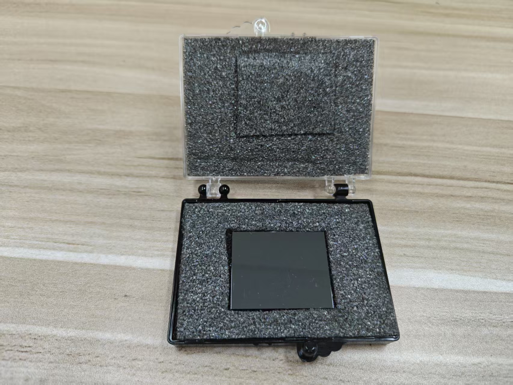
Achieving uniform electrode deposition on Cadmium Zinc Telluride (CZT) crystals is a critical challenge in the design and fabrication of high-performance radiation detectors. Since CZT is commonly used in X-ray and gamma-ray detection, the quality of the electrode layer directly affects the detector's charge collection efficiency, energy resolution, and overall performance. Inconsistent electrode deposition can lead to uneven charge collection, higher leakage currents, and poor energy resolution. Several factors contribute to the difficulty in achieving uniform electrode deposition on CZT crystals, ranging from material properties and surface characteristics to deposition methods and process control.
## Surface Roughness and Crystal Structure
One of the primary challenges in achieving uniform electrode deposition on CZT crystals is the surface roughness and crystal structure of the CZT material. CZT crystals, like many semiconductor materials, can have inherent surface defects, grain boundaries, and uneven topography, which can affect how an electrode layer adheres and spreads across the surface. These structural variations can cause non-uniform deposition, leading to regions of weak electrical contact and inconsistent charge collection.
Moreover, surface contamination or oxidation of CZT surfaces can alter the interface properties, further complicating the deposition process. For example, oxidation of the surface can create an increased resistance to electrode adhesion, resulting in poor quality coatings or patchy deposition.
## Deposition Techniques and Control
The method used for electrode deposition plays a significant role in determining the uniformity of the layer. Common techniques for electrode deposition on CZT include sputtering, evaporation, chemical vapor deposition (CVD), and electroplating. Each of these methods presents unique challenges in achieving uniform coverage:
* Sputtering involves bombarding the target material with ions, causing the material to sputter onto the surface. While it can provide thin, uniform layers, non-uniform ion distribution or substrate heating can lead to uneven deposition. Achieving uniform sputtering requires precise control over power settings, gas flow rates, and substrate positioning.
* Evaporation involves heating the electrode material until it evaporates and condenses onto the CZT surface. While evaporation is often used to produce high-quality, thin films, achieving a uniform thickness across the entire surface of a CZT crystal is difficult due to the line-of-sight nature of the process. Variations in the distance between the evaporation source and the substrate can cause thicker deposition in some areas and thinner deposition in others.
* Chemical Vapor Deposition (CVD) is another deposition method used for creating electrode layers. It relies on the chemical reaction of precursor gases to deposit materials onto the surface. While CVD can provide high-quality uniform films, it requires precise temperature control and gas distribution. Non-uniform gas flow or temperature gradients can cause localized variations in deposition rates, leading to non-uniform films.
* Electroplating is a wet process used for electrode deposition where an electrode material is deposited onto the surface by applying a voltage to an electrolyte solution. The challenge with electroplating is maintaining a constant current density across the surface, as non-uniform current distribution can result in thicker areas near edges and thinner areas in the center, leading to non-uniform deposition.
## Thickness Control
Achieving precise thickness control across the entire surface of the CZT crystal is a significant challenge in electrode deposition. Thin films are required for optimal performance, but small variations in the deposition time, temperature, or power can result in uneven thickness, which may compromise the performance of the detector. Inconsistent thickness can lead to differing electric fields at different locations on the crystal, causing uneven charge collection and poor energy resolution.
For example, if one region of the crystal has a thicker electrode layer, it might result in higher capacitance, slower charge collection, and distorted signals. Conversely, thinner areas may not collect enough charge or cause poor contact, resulting in low efficiency.
## Substrate Heating and Thermal Effects
During the deposition process, thermal effects play a crucial role in achieving uniform electrode layers. Many deposition techniques, such as evaporation and sputtering, generate significant heat during processing. This heat can cause thermal expansion of the CZT substrate, which may lead to distortions in the crystal structure, creating uneven surfaces that affect the deposition uniformity.
For instance, uneven heating of the substrate can cause warping or buckling of the crystal, leading to inconsistent deposition. Additionally, thermal gradients across the surface can cause variations in the deposition rate, leading to non-uniform electrode layers.
## Adhesion and Interface Properties
The adhesion of the electrode material to the CZT crystal surface is another challenge that affects the uniformity of the deposited electrode. If the surface is not properly cleaned or passivated, the electrode material may fail to adhere uniformly or peel off in certain areas. Inadequate adhesion can lead to poor contact quality, which negatively affects charge collection efficiency.
Moreover, interface properties such as the presence of surface oxides, contaminants, or grain boundaries on the CZT surface can lead to inconsistent deposition. Some areas of the surface may exhibit stronger adhesion, leading to thicker deposits, while other areas may show weaker adhesion, resulting in thin or patchy coatings.
## Contamination and Impurities
Contamination and impurities are common obstacles in achieving uniform electrode deposition on CZT crystals. Particulate matter, dust, or foreign substances on the surface of the crystal can cause irregularities in the deposition process. Even trace amounts of contamination can lead to local changes in deposition rate or chemical reactivity, resulting in non-uniform electrode layers.
To mitigate these effects, cleanroom environments and precise surface preparation techniques are required to minimize contamination during the deposition process. Chemical cleaning, plasma etching, or surface passivation can help ensure a clean and uniform surface for deposition.
## Strain and Stress in Electrode Layers
Strain and stress in the electrode material itself can affect uniformity during deposition. For instance, stressed layers can lead to poor film adherence, delamination, or uneven surface morphology. Thermal expansion mismatches between the CZT crystal and the electrode material can introduce mechanical stress, causing the electrode layer to crack or distort, resulting in non-uniform deposition and poor performance.
## Conclusion
Achieving uniform electrode deposition on CZT crystals is fraught with challenges related to surface characteristics, deposition methods, thickness control, and material interactions. Factors such as surface roughness, deposition technique, adhesion properties, and thermal effects all contribute to the difficulty in ensuring a consistent electrode layer. Overcoming these challenges requires precise process control, cleanroom environments, and careful selection of deposition methods to achieve high-quality, uniform electrode deposition. Uniform electrodes are crucial for ensuring optimal performance, including high charge collection efficiency, low leakage current, and improved energy resolution in CZT-based radiation detectors.
CdZnTe Association (CdZnTe.com)
https://www.cdznte.com/blog/what-are-the-challenges-in-achieving-uniform-electrode-deposition-on-czt-crystals.html