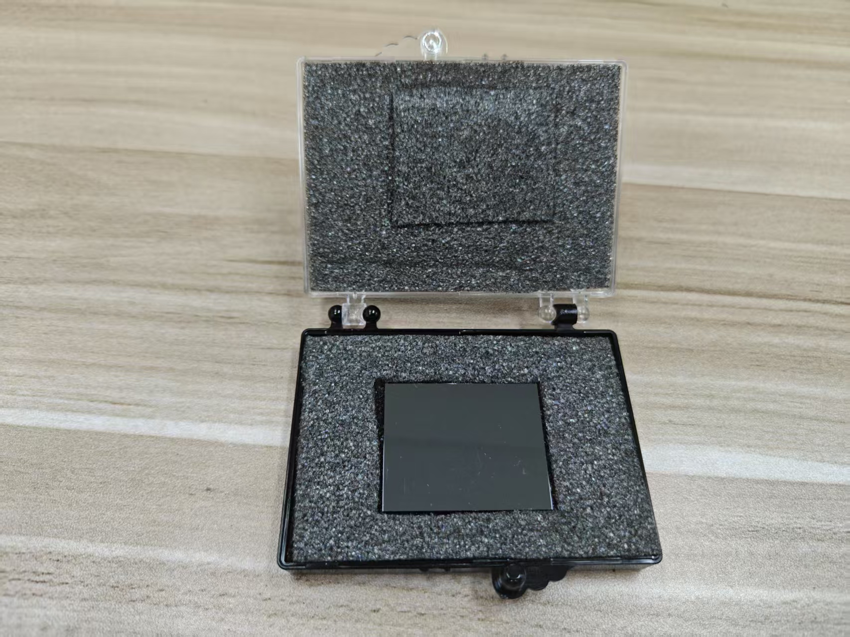
## Challenges in Cutting and Polishing CZT Crystal for High-Precision Applications
Cutting and polishing
Cadmium Zinc Telluride (CZT) crystals for high-precision applications, such as
detectors and
semiconductor devices, presents several challenges due to the unique material properties of CZT. These challenges can affect the crystal's performance, particularly in terms of
surface quality,
mechanical integrity, and
optical characteristics. The following are the key challenges encountered when processing CZT crystals for high-precision applications:
## 1. Brittleness and Fragility of CZT Crystals
CZT crystals are inherently
brittle and
fragile, making them prone to
fracture during the cutting and polishing processes. The crystal's tendency to crack or shatter when subjected to mechanical stress is a significant challenge in manufacturing high-quality components.
*
Cleavage Planes: CZT crystals have well-defined cleavage planes, which can cause
controlled fracture along specific planes. This characteristic is both advantageous and problematic. While cleavage can sometimes help in cutting along certain planes, it can also lead to unintentional fractures during machining if the cut is not precisely aligned with the crystal’s natural fracture lines.
*
Handling and Stress Management: Proper handling of CZT crystals is critical to prevent the introduction of
microfractures or
surface damage, especially during the cutting and polishing phases. Crystals must be handled with care, using soft tools and minimal force to avoid generating stresses that could lead to breakage.
## 2. Challenges in Achieving High-Quality Surface Finish
Polishing CZT crystals to achieve a
smooth and
optically flat surface is essential for high-precision applications. However, the unique material properties of CZT make this process complex:
*
Surface Roughness: Achieving a
low surface roughness is critical for applications such as
detector windows or
optical components, where imperfections can affect the performance, including
signal clarity and
energy resolution. The polishing process must be carefully controlled to minimize
scratches,
micro-cracks, and
surface contamination, which can significantly impact the crystal’s properties.
*
Surface Contamination: CZT crystals are sensitive to surface contamination during the cutting and polishing process. Any residues from polishing compounds, abrasives, or environmental contaminants can introduce unwanted
impurities into the crystal, which can negatively affect
carrier mobility,
recombination rates, and the
performance of CZT-based devices. Therefore, cleaning processes must be rigorously controlled.
*
Optical and Electrical Property Preservation: The polishing process must ensure that the
electrical and
optical properties of the CZT crystal are not compromised. Over-polishing can lead to a loss of critical material characteristics, such as
carrier lifetimes or
bandgap properties.
## 3. Non-Uniformity and Inhomogeneity of Crystal Growth
CZT crystals, especially those grown by
VGF (Vertical Gradient Freeze) or
Bridgman techniques, can exhibit
inhomogeneities and
structural defects due to
temperature gradients,
composition variations, and
segregation of elements during the crystal growth process. These inhomogeneities can make the cutting and polishing processes more challenging:
*
Variation in Hardness: Due to the inhomogeneous distribution of
cadmium and
zinc in the crystal lattice, certain areas of the CZT crystal may be softer or harder than others, leading to
uneven polishing. This can result in a
non-uniform surface and
differential wear of polishing tools, affecting the final surface quality.
*
Internal Defects: Internal defects such as
dislocations,
vacancies, or
precipitates can also lead to
non-uniform machining behavior. For instance, areas of the crystal with high defect density may be more difficult to cut or polish, resulting in
surface roughness or
chipping in these regions.
## 4. Thermal Management During Cutting and Polishing
Both the cutting and polishing processes generate
heat, which can adversely affect the CZT crystal, especially given its
high thermal expansion coefficient and relatively
low thermal conductivity compared to other materials like silicon or germanium.
*
Heat-Induced Damage: Excessive heat can cause
thermal stress or even
melting of the CZT crystal, leading to
surface degradation. In particular, localized heating can cause
cracking,
warping, or
deformation, which compromises the crystal’s performance. Careful temperature management and cooling systems are required to minimize these risks during machining.
*
Tool Wear and Efficiency: High-speed cutting tools and polishing pads can also generate heat, which might reduce the
efficiency of material removal. This makes it essential to carefully control the
cutting speed,
pressure, and
lubrication to prevent
thermal damage.
## 5. Alignment and Precision in Cutting
For high-precision applications, it is crucial to align the cutting planes correctly with respect to the crystal’s
crystallographic axes. Misalignment can result in:
*
Distortion of Electrical Properties: The performance of a CZT-based detector can be severely impacted if the cut is made at the wrong angle relative to the crystal's inherent properties. For instance, misaligning the crystal’s axes can introduce
strain and cause
anisotropic behavior in the crystal, which affects
charge transport and
detection efficiency.
*
Angle-Dependent Properties: CZT crystals are known to exhibit
anisotropic behavior, meaning their physical and electrical properties can vary depending on the direction along the crystal axes. Thus, precision in cutting and polishing, ensuring that the crystal is correctly oriented, is critical to maintaining optimal performance.
## 6. Time-Consuming and Expensive Processes
Both
cutting and
polishing of CZT crystals require a significant investment of time and resources. The
cost of tools,
abrasives, and
polishing compounds can be high, especially when used in
large-scale production. Furthermore, the process often requires multiple stages of
finishing to achieve the desired surface quality:
*
Multiple Polishing Stages: Achieving a high-quality finish on a CZT crystal often requires
several steps of polishing, with increasingly finer abrasives. Each stage adds time and complexity to the process.
*
Yield Loss: Due to the brittleness and fragility of CZT crystals, there is always a risk of
material waste during cutting and polishing. If the crystal breaks or is damaged, it can result in
yield loss, making the process
inefficient and costly.
## 7. Challenges in Polishing Small Features or Pixel Arrays
In applications where
pixelated arrays or
microscale features are needed, polishing becomes even more challenging:
*
Small-Scale Polishing: Polishing
micro-scale features on CZT crystals, such as in
detector arrays or
microscale devices, requires extremely fine control over the polishing process. Traditional polishing techniques may not be suitable for achieving the
sub-micron surface finishes required for these high-precision applications.
*
Uniformity Across Pixels: In
pixelated detectors or
multi-element arrays, achieving uniformity in the polishing process is essential to ensure
uniform response across all pixels. Any inconsistencies in surface finish or depth can result in
non-uniform performance, reducing the accuracy of the system.
## 8. Environmental Sensitivity
CZT crystals are sensitive to
humidity and
environmental contamination. During the cutting and polishing processes, the crystal can absorb moisture or react with airborne
contaminants, leading to
oxidation or the formation of
surface states. These environmental factors can degrade the quality of the polished surface and affect the crystal’s
electrical properties, making it critical to carry out the polishing process in a
controlled environment.
## 9. Summary
The challenges in cutting and polishing CZT crystals for high-precision applications stem from a combination of material properties, handling difficulties, and the need for exacting precision. The main challenges include:
1.
Brittleness and fragility leading to the risk of fracture and material loss.
2.
Difficulties in achieving a high-quality surface finish without introducing scratches or defects.
3.
Inhomogeneities in crystal growth that cause non-uniformities in hardness and defect distribution.
4.
Thermal stress generated during cutting and polishing processes.
5.
Alignment issues due to the anisotropic nature of CZT crystals.
6. The
costly and time-consuming nature of the polishing process, especially for large-scale or high-precision production.
7.
Challenges in processing small-scale features or pixel arrays for detectors.
To overcome these challenges, precise control over the machining parameters, careful handling, and optimized tool selection are necessary to achieve the desired high-quality surface finish without compromising the performance of the CZT crystal.
CdZnTe Association (CdZnTe.com)
https://www.cdznte.com/blog/what-are-the-challenges-in-cutting-and-polishing-czt-crystal-for-high-precision-applications.html