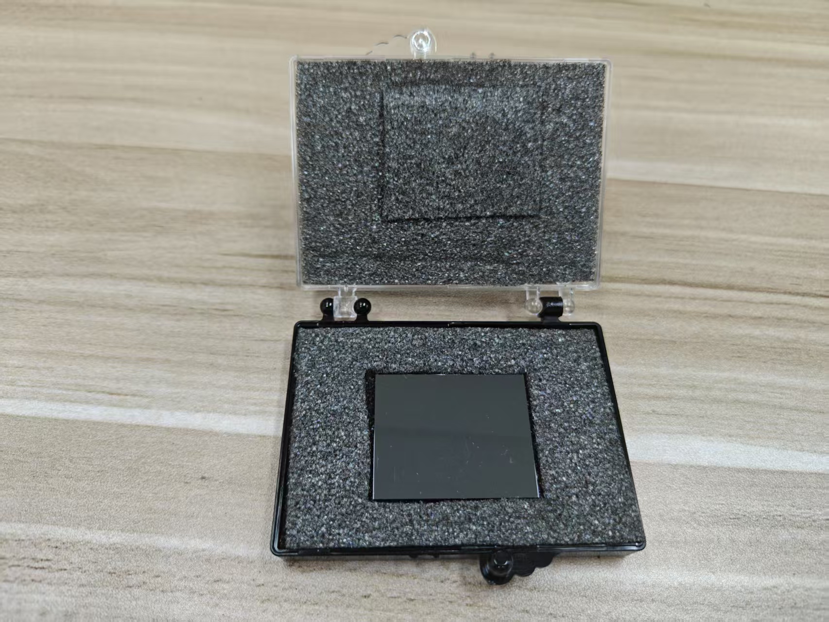
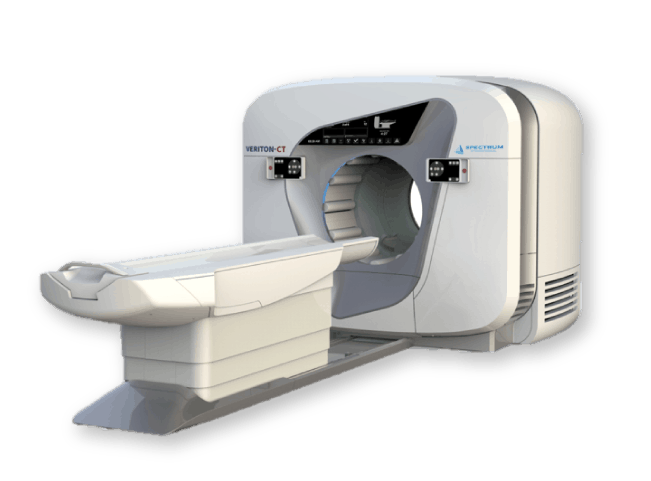
What are the dominant types of deep-level defects in CSS-grown CdZnTe films, and how do they affect carrier trapping?

Blog / Date: July 25, 2025 / Author: CdZnTe.com / Hits: 57
What are the dominant types of deep-level defects in CSS-grown CdZnTe films, and how do they affect carrier trapping?
In Close-Spaced Sublimation (CSS)-grown CdZnTe (CZT) films, the process of material growth often leads to the formation of various deep-level defects. These defects can have a significant impact on the material's carrier transport properties, particularly by introducing trapping centers that reduce the mobility and lifetime of charge carriers. The dominant types of these deep-level defects and their effects on carrier trapping are summarized below.

## 1. Te Vacancy (V\_Te)


## Characteristics and Formation:


* Te vacancies (V\_Te) are one of the most common deep-level defects in CZT films, particularly in Te-rich growth conditions, which are typical of CSS growth.
* These vacancies arise when Te atoms are missing from the crystal lattice. V\_Te can act as a trap for both electrons and holes depending on the material's doping and carrier concentration.

## Effect on Carrier Trapping:


* V\_Te creates deep trap states within the band gap, usually near the mid-gap region. These states can capture carriers, particularly electrons, and prevent them from contributing to electrical conduction or radiation detection performance.
* The capture cross-section of V\_Te is large, which means that these defects significantly reduce carrier lifetime (τ) and increase recombination rates, leading to lower device efficiency.
* In detectors, the presence of V\_Te reduces charge collection efficiency, particularly in radiation detection applications where the carrier lifetime is critical for the accurate measurement of ionizing radiation.

## 2. Cd Vacancy (V\_Cd)


## Characteristics and Formation:


* Cd vacancies (V\_Cd) are another type of deep-level defect that can form in CSS-grown CZT films.
* They are typically created under Cd-poor growth conditions, where there is an imbalance between the Cd and Te stoichiometry during film deposition.

## Effect on Carrier Trapping:


* V\_Cd is a donor-type defect, and it introduces shallow donor states in the band gap, often close to the conduction band.
* These states can donate electrons to the conduction band, increasing the free electron concentration in the material, which may lead to n-type conductivity.
* V\_Cd can act as a trap for holes, but its effect on electron trapping is less significant than that of V\_Te. In some cases, it can also contribute to compensating acceptor states, affecting carrier concentration and material resistivity.

## 3. Te-Cd Antisite Defects (Te\_Cd and Cd\_Te)


## Characteristics and Formation:


* Te-Cd antisites (Te\_Cd) and Cd-Te antisites (Cd\_Te) are formed when Te atoms occupy Cd sites or Cd atoms occupy Te sites in the crystal structure.
* These antisite defects are prevalent in non-stoichiometric CZT films, particularly in conditions where the Te/Cd ratio is skewed, leading to a higher concentration of Te.

## Effect on Carrier Trapping:


* Te\_Cd is an acceptor-type defect, creating trap states that can capture electrons, leading to compensated conduction and reduced carrier mobility.
* Cd\_Te is a donor-type defect and can trap holes, similarly impacting carrier mobility but less significantly than Te\_Cd.
* Both types of antisite defects contribute to carrier recombination and lower efficiency in radiation detection, where long carrier lifetimes are required for high-quality signal detection.

## 4. Interstitial Defects (Cd\_i and Te\_i)


## Characteristics and Formation:


* Interstitial defects such as Cd\_i (cadmium interstitials) and Te\_i (tellurium interstitials) arise when atoms occupy sites in the crystal lattice that are not part of the normal atomic arrangement.
* These defects can form during the CSS growth process due to high deposition rates and thermal gradients that can cause atomic displacements.

## Effect on Carrier Trapping:


* Cd\_i and Te\_i can create shallow traps for carriers, particularly electrons and holes. These defects can act as scattering centers and lead to increased carrier recombination.
* Interstitials may have a high activation energy for trapping, but at high concentrations, they still significantly reduce carrier mobility by introducing localized potential fluctuations in the material.

## 5. Dislocation-Related Defects


## Characteristics and Formation:


* Dislocations are another common defect in CSS-grown CZT films, particularly because the lattice mismatch between the CZT film and GaAs substrate can cause the formation of misfit dislocations during film growth.
* These dislocations introduce strain fields and line defects that contribute to point defects in the material.

## Effect on Carrier Trapping:


* Dislocations often introduce localized energy levels within the band gap, which can act as recombination centers or traps for both electrons and holes.
* The presence of dislocation-related traps decreases carrier lifetime and charge transport efficiency, leading to poor performance in applications such as radiation detection, where the fast collection of charge carriers is essential.

## 6. Impurities and Dopants


## Characteristics and Formation:


* Impurities such as Cu, Fe, and other metal contaminants can enter the CZT film during the CSS growth process, either from the environment or the raw materials.
* Dopants, such as Al or In, may also be intentionally introduced to modify the electronic properties of the CZT film.

## Effect on Carrier Trapping:


* Impurities and dopants can create deep-level traps in the band gap, often leading to unwanted carrier recombination.
* Transition metal impurities, in particular, can form donor or acceptor states at deep levels within the band gap, which can lead to trap-assisted recombination and carrier trapping.
* Although dopants like Al and In are sometimes used to improve material properties, they can also introduce new shallow or deep-level defects that can have negative effects on the carrier transport properties.

## 7. Impact on Carrier Transport and Device Performance


## Carrier Trapping in Radiation Detectors


The presence of deep-level defects such as vacancies, antisites, and dislocations significantly impacts the performance of radiation detectors based on CZT films. Carrier trapping at these defects leads to:

* Increased recombination rates, lowering the carrier lifetime (τ) and reducing the (μτ)\_e product, which is critical for efficient charge collection in detectors.
* Reduced charge collection efficiency, especially in the case of high-energy radiation detection, where long carrier lifetimes are essential for the accurate measurement of energy.
* Lower resolution in imaging or spectroscopy applications, as the trapped charge carriers reduce the effectiveness of signal readout.

## Overall Effect on Device Efficiency


In summary, deep-level defects in CSS-grown CZT films have a major impact on carrier trapping and recombination, reducing carrier mobility, lifetime, and overall device efficiency. The primary deep-level defects, such as Te vacancies, Cd vacancies, antisites, and dislocations, all contribute to trapping centers that impair the material's electrical and optical properties. Reducing the concentration of these defects, through improved growth conditions, annealing, or material optimization, is essential for improving the performance of CZT-based detectors and other optoelectronic applications.


CdZnTe Association (CdZnTe.com)
https://www.cdznte.com/blog/what-are-the-dominant-types-of-deep-level-defects-in-css-grown-cdznte-films-and-how-do-they-affect-carrier-trapping.html
CZT Detectors
Collection of a curated range of high-performance cadmium zinc telluride (CZT) radiation detectors for medical, security, and scientific applications