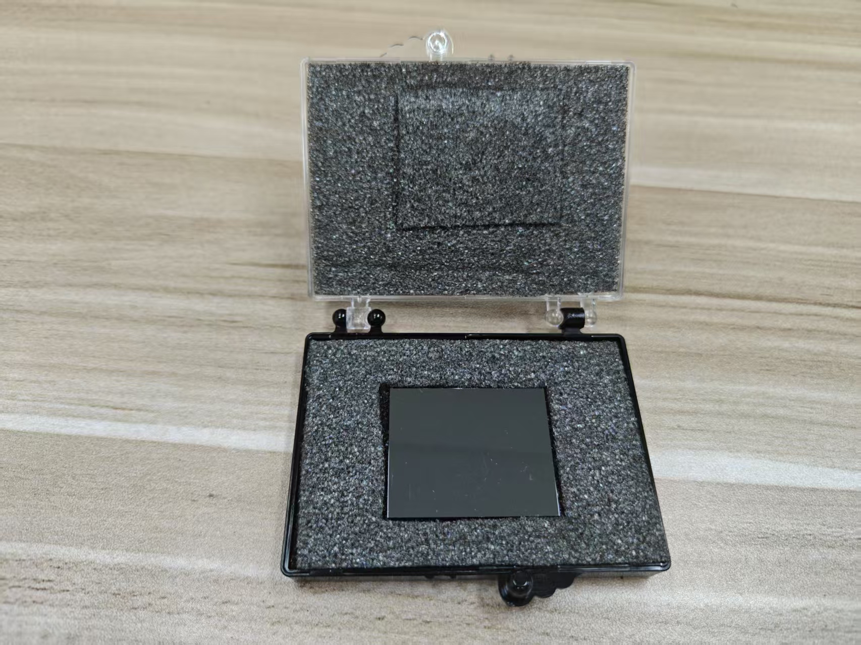
## Introduction
Reducing pixel-to-pixel variation in CZT pixeled arrays is crucial for achieving high-performance and consistent detection in high-energy photon applications, such as gamma-ray and X-ray detection. Variations in performance between individual pixels can arise from inconsistencies in the CZT crystal growth, pixel fabrication, and electrode deposition processes. These variations can degrade spatial resolution, energy resolution, and overall detection efficiency, which are essential for applications requiring accurate imaging and precise measurements. To minimize pixel-to-pixel variations, several techniques can be employed at different stages of the CZT pixeled array fabrication process. This article discusses the most effective methods for reducing pixel-to-pixel variation in CZT detectors.
## 1. Improved Crystal Growth Techniques
The quality and uniformity of the CZT crystal are the most fundamental factors influencing pixel-to-pixel variation. The growth process must be carefully controlled to ensure homogeneity across the entire crystal, as even slight differences in crystal properties can lead to significant variations in detector performance.
* Vertical Bridgman method: This is a commonly used method for growing CZT crystals. By carefully controlling the temperature gradients and doping levels during the growth process, it is possible to reduce the formation of defects and ensure that the CZT crystal is uniform throughout. This method helps minimize pixel-to-pixel variation by producing a more consistent material quality across the detector.
* High-pressure direct crystallization (HPDC): In this method, CZT is grown under high pressure, which can lead to larger and more uniform crystals. HPDC reduces defects and ensures that the CZT material is less susceptible to inhomogeneities in terms of doping concentration, crystal orientation, and electron mobility, all of which contribute to pixel-to-pixel variation.
By improving the crystal growth process, the material’s electrical properties become more uniform, resulting in more consistent performance across individual pixels in the array.
## 2. Optimization of Pixel Design
The pixel design—specifically, the geometry and spacing of the pixels—has a significant impact on pixel-to-pixel variation in CZT pixeled arrays. Variations in pixel size, shape, and arrangement can lead to differences in charge collection efficiency and spatial resolution.
* Uniform pixel pitch: Ensuring that the pixel pitch (the distance between adjacent pixels) is consistent across the array is essential for reducing variation. Irregular pixel spacing can lead to non-uniform electric fields, which may cause variation in charge collection efficiency. Using advanced photolithography or e-beam lithography techniques can help to achieve precise pixel placement and reduce variation between pixels.
* Hexagonal vs. square pixels: Hexagonal pixel arrangements can minimize edge effects and reduce non-uniformities that may occur with square pixels. In certain configurations, hexagonal pixels can help achieve more uniform charge collection across the array, reducing the variation in performance between adjacent pixels.
By carefully designing the pixel structure and ensuring uniformity in pixel pitch, spatial resolution can be improved, and pixel-to-pixel variation can be minimized.
## 3. Electrode Deposition Techniques
The electrode material and the deposition process significantly affect the interface between the electrode and the CZT crystal. Variations in electrode thickness, adhesion, and patterning can cause differences in charge collection efficiency and contact resistance between individual pixels.
* Sputtering: Sputtering is a widely used method for depositing thin-film electrodes on CZT. It offers better uniformity and adhesion compared to other deposition methods like evaporation. By using reactive sputtering with a controlled deposition rate, it is possible to achieve uniform electrode coverage, reducing pixel-to-pixel variation in charge collection and signal generation.
* Electron-beam evaporation: This method is another common way to deposit metal electrodes on CZT crystals. By optimizing deposition parameters, such as the deposition rate, angle, and temperature, uniform coverage of the electrode material can be achieved, helping to minimize variation in the interface between the pixel and the CZT crystal.
* Electrode material choice: Selecting a high-quality electrode material with good conductivity, such as gold (Au) or platinum (Pt), ensures a low contact resistance and stable electrical contact between the electrode and CZT. Consistent electrode properties across all pixels are essential for minimizing performance variation in the array.
By optimizing the electrode deposition process, uniform charge collection and low contact resistance can be achieved, reducing pixel-to-pixel variation in the CZT pixeled array.
## 4. Surface Treatment and Passivation
Surface treatment techniques can significantly improve the interface quality between the CZT crystal and the electrode, reducing surface defects that can lead to pixel-to-pixel variation. These treatments help to passivate the CZT surface, enhancing its electrical performance.
* Surface cleaning: Before electrode deposition, it is crucial to ensure that the CZT crystal surface is free of contaminants such as organic residues, dust, or oxidation. Techniques like plasma cleaning or chemical cleaning can be used to remove surface contaminants, ensuring better electrode adhesion and reducing performance variation across pixels.
* Passivation layers: Applying a passivation layer to the CZT surface can help to prevent surface states from trapping charge carriers, which can lead to charge loss and variation in detector performance. Materials like silicon nitride (Si₃N₄) or silicon dioxide (SiO₂) are commonly used for passivating the surface. This layer can help to smooth out the interface and improve charge transport, reducing pixel-to-pixel differences in performance.
By ensuring that the CZT crystal surface is free of defects and contaminants, and by applying passivation layers, the interface quality between the pixel and the crystal is improved, reducing pixel-to-pixel variation.
## 5. Thermal Management and Control
Temperature fluctuations during fabrication and operation can exacerbate pixel-to-pixel variation in CZT pixeled arrays. Thermal effects can influence charge transport, doping concentration, and electrode adhesion, leading to non-uniform performance across the detector.
* Controlled crystal growth environment: Maintaining a uniform temperature during the CZT crystal growth process is crucial to ensure that the material properties are consistent across the entire crystal. By using temperature-controlled furnaces and high-pressure systems, variations in doping levels and charge transport properties can be minimized.
* Active thermal management: During operation, using temperature regulation systems such as Peltier coolers or cryostats can help maintain the CZT pixeled array at a stable operating temperature. This ensures that the detector performance remains consistent across all pixels, reducing the effects of thermal gradients that could cause pixel-to-pixel variations.
By maintaining temperature stability throughout the manufacturing process and during operation, thermal effects can be minimized, reducing pixel-to-pixel variation in the detector.
## 6. Calibration and Compensation Techniques
After the CZT pixeled array is fabricated, calibration and compensation techniques can be used to correct for pixel-to-pixel variation that might still exist. These techniques help ensure that the detector provides uniform performance across the array.
* Energy calibration: Energy calibration can be used to correct for variations in energy resolution across the pixels. By measuring the detector's response to known calibration sources (e.g., Cs-137, Co-60), corrections can be applied to compensate for pixel-to-pixel variation in energy measurement.
* Pixel-specific corrections: In cases where variation exists between individual pixels, pixel-specific compensation can be applied through digital signal processing. This can involve adjusting the signals from individual pixels to account for any discrepancies in charge collection or noise levels, ensuring that the overall array provides consistent performance.
By applying calibration and compensation methods, residual pixel-to-pixel variations can be minimized, ensuring that the CZT pixeled array operates with uniform performance.
## Conclusion
Reducing pixel-to-pixel variation in CZT pixeled arrays is essential for ensuring uniform detection efficiency, high spatial and energy resolution, and consistent performance across the entire detector. Key methods to reduce variation include improving the crystal growth process, optimizing pixel design, utilizing uniform electrode deposition techniques, applying surface treatments, managing thermal effects, and using calibration and compensation techniques. By addressing these factors, the CZT pixeled arrays can achieve high-quality performance, making them suitable for a wide range of applications in high-energy photon detection.
CdZnTe Association (CdZnTe.com)
https://www.cdznte.com/blog/what-are-the-most-effective-methods-for-reducing-pixel-to-pixel-variation-in-czt-pixeled-arrays.html