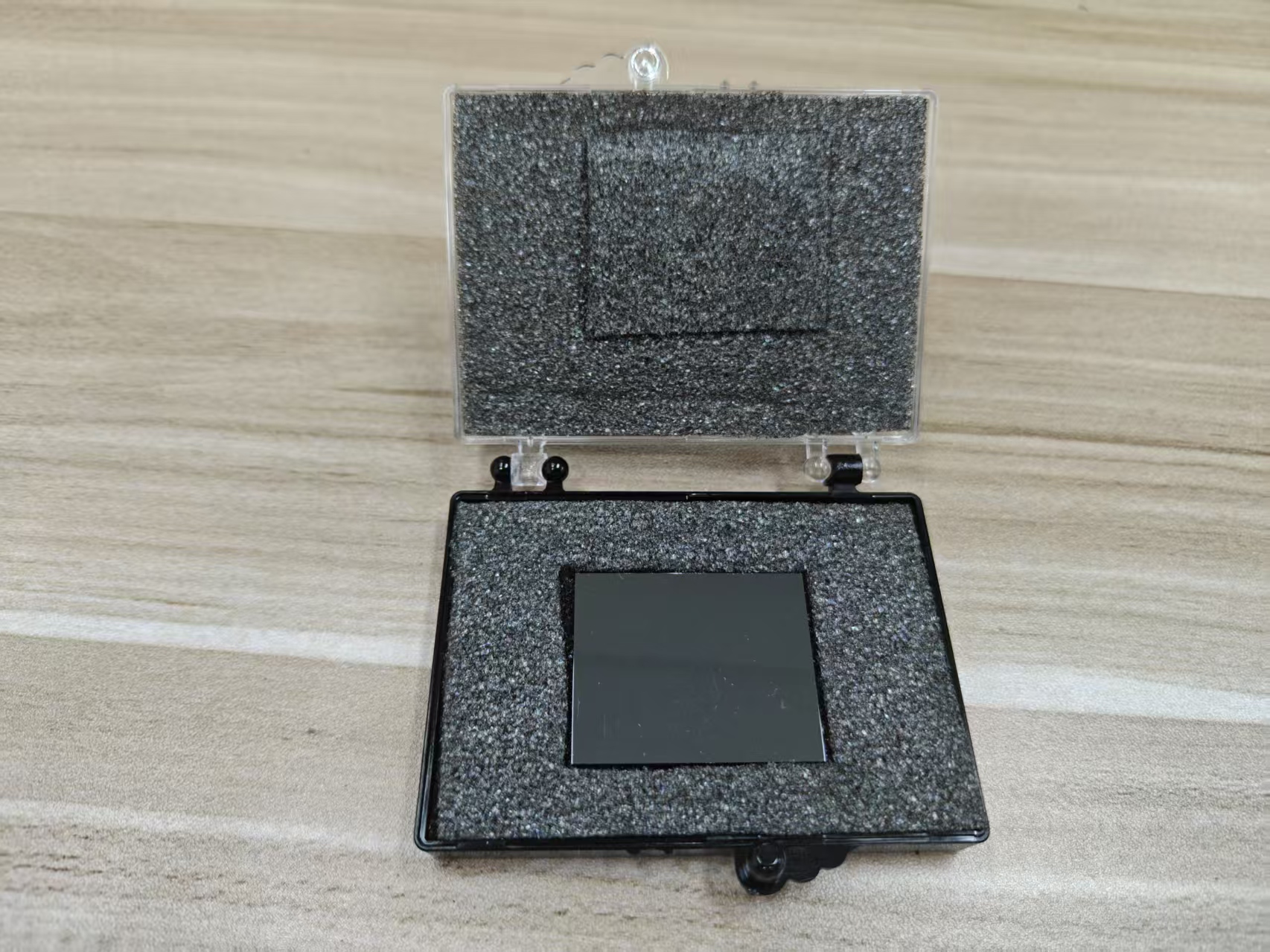
## Introduction
The deposition of thin-film electrodes on Cadmium Zinc Telluride (CZT) crystals is a critical step in the fabrication of CZT-based radiation detectors. The performance of these detectors is highly dependent on the quality and uniformity of the electrode material, as it directly influences charge collection efficiency, leakage currents, and overall detector stability. Thin-film deposition techniques must ensure that the electrodes have a smooth, uniform surface with a strong electrical contact to the CZT crystal, while minimizing the formation of defects or surface contamination that can degrade performance. Several deposition techniques are commonly used for thin-film electrode formation, each with its advantages and challenges depending on the specific application and material compatibility.
## Sputtering
Sputtering is one of the most widely used techniques for depositing thin-film electrodes on CZT crystals. It involves the bombardment of a target material with energetic particles (typically argon ions), causing atoms from the target to be ejected and deposited onto the surface of the CZT crystal.
* Advantages:
* High-quality films: Sputtering produces dense, uniform films with good adhesion to the substrate. It is particularly effective for depositing metals like gold, platinum, and silver, which are commonly used as electrodes in CZT detectors.
* Precise control: The film thickness and composition can be controlled with high precision, allowing for optimized electrode properties.
* Low contamination: Sputtering can be performed in a vacuum environment, reducing the risk of contamination from the atmosphere.
* Challenges:
* Stress in thin films: Depending on the deposition parameters, sputtered films may experience internal stress due to the high-energy particle bombardment, which can lead to film cracking or delamination if not properly managed.
* Target material compatibility: Sputtering may require specialized target materials, and the interaction between the sputtered material and the CZT surface may need to be optimized to ensure good adhesion.
In the case of CZT crystals, reactive sputtering (using reactive gases such as oxygen or nitrogen) may be required to improve the adhesion and electrical properties of the deposited electrode layer, particularly if oxide formation or material reactivity is a concern.
## Electron Beam (e-beam) Evaporation
Electron beam (e-beam) evaporation is another widely used deposition technique in the fabrication of thin-film electrodes. In this process, an electron beam is directed at a target material (typically a metal), causing it to evaporate and condense onto the CZT crystal substrate.
* Advantages:
* High deposition rate: E-beam evaporation is capable of high deposition rates, which can be advantageous when a thick electrode layer is needed in a short amount of time.
* Low temperatures: This method can be performed at relatively low temperatures, which is beneficial for sensitive substrates like CZT, which may degrade at higher temperatures.
* Good uniformity: The films produced by e-beam evaporation are often smooth and uniform, especially when thermal evaporation is controlled.
* Challenges:
* Limited material choices: E-beam evaporation typically works best for metallic materials and may not be suitable for all electrode materials (e.g., some alloys or compounds).
* Thermal effects: There can be localized heating of the substrate during the deposition process, which might affect the CZT crystal and lead to crystallization or deformation if not controlled carefully.
For CZT detectors, gold and platinum are often used in e-beam evaporation due to their stability, electrical conductivity, and compatibility with the CZT crystal.
## Thermal Evaporation
Thermal evaporation involves the heating of a material until it evaporates, and then the vapor is allowed to condense on the surface of the CZT crystal. This method is similar to e-beam evaporation but uses resistive heating to evaporate the material.
* Advantages:
* Simplicity: Thermal evaporation is a relatively simple technique that can be used to deposit thin films of various materials, including gold, silver, aluminum, and nickel.
* Low equipment cost: Compared to other techniques, thermal evaporation systems are generally less expensive and easier to operate.
* Challenges:
* Limited material versatility: Like e-beam evaporation, thermal evaporation is most effective for metallic films, but it may not be suitable for complex alloy films or oxide layers.
* Lower deposition rates: Compared to sputtering or e-beam evaporation, thermal evaporation typically has a lower deposition rate, which can be a limitation in some applications.
Thermal evaporation is often used for the deposition of gold and silver electrodes on CZT due to their high conductivity and stability.
## Pulsed Laser Deposition (PLD)
Pulsed Laser Deposition (PLD) is a high-energy deposition method in which a laser pulse is used to ablate material from a target, which is then deposited as a thin film on the CZT crystal substrate.
* Advantages:
* Material versatility: PLD can be used to deposit a wide range of materials, including metals, oxides, and alloys, making it highly versatile for electrode formation.
* Precise control: The deposition process can be finely tuned, allowing for the precise control of film thickness, composition, and microstructure.
* High-quality films: PLD produces films that often have excellent adhesion to the substrate and can have controlled stoichiometry.
* Challenges:
* Complexity and cost: PLD systems tend to be more expensive and require specialized equipment compared to simpler techniques like thermal evaporation or sputtering.
* Substrate heating: The laser pulses may generate significant heat, which can affect the CZT substrate if not carefully controlled.
PLD is typically used for the deposition of oxide-based electrodes or alloy electrodes, where precise control of the film composition and stoichiometry is required.
## Chemical Vapor Deposition (CVD)
Chemical Vapor Deposition (CVD) is a deposition technique that involves the reaction of gaseous precursors in a chamber to form a solid film on the substrate. This technique is widely used for depositing thin films of metals, semiconductors, and oxides.
* Advantages:
* Uniform coverage: CVD is particularly effective for depositing films with uniform coverage on complex or uneven surfaces, which is essential for achieving high-quality electrodes on CZT crystals.
* Conformal coatings: CVD allows for conformal coatings, ensuring that the entire surface of the CZT crystal is covered by a thin electrode layer, which is essential for consistent charge collection.
* Challenges:
* Material compatibility: CVD may not always be compatible with all electrode materials, especially metals like gold or platinum, which may require different precursor chemicals.
* Temperature sensitivity: Some CVD processes require high temperatures, which could affect the CZT crystal’s stability if not carefully controlled.
CVD is often used for dielectric films or metal oxide layers but can also be used for depositing electrode materials if the material’s precursors are available.
## Atomic Layer Deposition (ALD)
Atomic Layer Deposition (ALD) is an advanced deposition technique that involves the sequential deposition of atomic layers to create extremely thin and uniform films.
* Advantages:
* Atomic precision: ALD allows for the deposition of highly uniform and atomic-scale thin films, making it ideal for creating high-quality electrodes on CZT crystals.
* Conformal coating: ALD ensures conformal coatings on substrates with complex or irregular geometries, which is useful when working with CZT crystals that may have rough surfaces or varied geometries.
* Challenges:
* Slow deposition rate: ALD is a slow process compared to other techniques like sputtering or thermal evaporation, which can be a limitation when faster deposition is required.
* Limited material options: ALD is typically used for depositing oxides or thin films of certain metals, and may not be suitable for all electrode materials used in CZT-based detectors.
ALD is generally used for depositing ultrathin dielectric layers or conductive materials, but its application for metal electrodes may be limited compared to sputtering or e-beam evaporation.
## Conclusion
The choice of deposition technique for thin-film electrode formation on CZT crystals depends on various factors, including the desired material, film thickness, uniformity, and process control. Sputtering, electron beam evaporation, and thermal evaporation are commonly used for depositing metallic electrodes, while PLD, CVD, and ALD offer advantages for specialized applications requiring precise material control and uniformity. Each technique has its strengths and limitations, and the most effective method will depend on the specific needs of the CZT detector application, such as achieving high charge collection efficiency, low leakage currents, and long-term stability.
CdZnTe Association (CdZnTe.com)
https://www.cdznte.com/blog/what-deposition-techniques-are-most-effective-for-thin-film-electrode-formation-on-czt-crystals.html