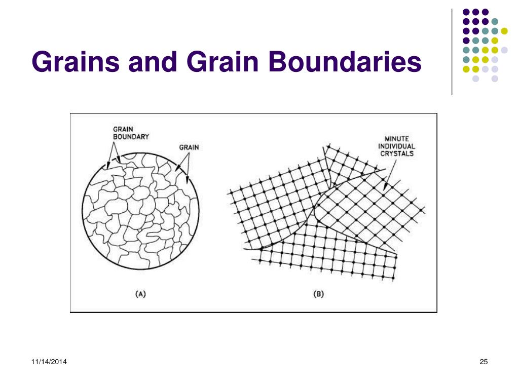
Grain boundaries play a critical role in determining the
performance of
Cadmium Zinc Telluride (CZT) detectors, influencing factors such as
charge collection efficiency,
energy resolution, and
overall detector stability. CZT, which is typically grown as
polycrystalline material in many detector applications, consists of a collection of
grains (small crystalline regions), each separated by
grain boundaries. These boundaries, while necessary for the polycrystalline structure, introduce a range of physical effects that can have both
positive and
negative impacts on the detector's
performance.
## 1. Impacts of Grain Boundaries on Charge Transport
## a. Charge Carrier Trapping
Grain boundaries can act as
trapping sites for charge carriers (electrons and holes). When an
electron-hole pair is generated by photon interaction within the crystal, the charge carriers need to travel toward the electrodes to produce a measurable signal. However, at the
grain boundaries, the crystal lattice is discontinuous, and defects or
dislocations can introduce localized
trap states. These traps can capture charge carriers, preventing them from reaching the electrodes, leading to
incomplete charge collection.
*
Increased Recombination: As the charge carriers are trapped at these sites, they can
recombine with their opposite charge, reducing the number of carriers that contribute to the current and signal. This recombination at grain boundaries
diminishes the charge collection efficiency (CCE) and ultimately reduces the
energy resolution of the detector.
## b. Reduced Charge Mobility
The
boundary regions often exhibit
disorder compared to the
bulk crystal. The lattice at grain boundaries may not be as well-aligned as in the bulk, and this
disorder introduces
scatterings and
resistive effects that hinder the mobility of the charge carriers. As a result, charge carriers may experience
slower drift velocities and more frequent
scattering events as they move through the crystal, particularly at
high bias voltages.
*
Charge Transport Inefficiency: Because grain boundaries are often more resistive and less conductive than the bulk of the material, charge carriers may
get stuck or be delayed at these regions. This impacts the overall
drift efficiency, meaning that the detector becomes less effective at collecting and separating charges, leading to
lower efficiency in radiation detection.
## 2. Electrical Heterogeneity at Grain Boundaries
## a. Increased Resistance
Grain boundaries often have different electrical properties compared to the bulk of the crystal, leading to
electrical inhomogeneity within the material. This heterogeneity can cause
local voltage drops and
non-uniform electric fields within the detector. As the grain boundaries have different electrical characteristics (due to differences in
doping,
crystal orientation, and
defect density), charge carriers may experience
uneven field strengths as they move through the crystal.
*
Field Distortion: The result is that some charge carriers may not experience the
strong uniform field needed to drift toward the electrodes efficiently. This can lead to a
distorted charge collection process, making it difficult to obtain accurate and precise measurements, especially for
high-energy photons.
## b. Junction Effects
In polycrystalline materials like CZT,
grain boundaries can form a series of
p-n junctions or
Schottky barriers, which can further impede the flow of charge carriers. These barriers can cause
partial charge blockages, especially if the grain boundaries contain high concentrations of
impurities or
defects. Such
junction effects further exacerbate the problem of
charge transport inefficiency and
polarization.
*
Carrier Rejection: In some cases, the grain boundaries can actually act as
barriers to charge flow, making it difficult for charge carriers to cross from one grain to another. This results in a
reduction in the overall conductivity of the material and a corresponding drop in the
charge collection efficiency.
## 3. Impact on Energy Resolution
One of the key performance metrics for
CZT detectors is their
energy resolution, which is a measure of the detector's ability to distinguish between different radiation energies. The presence of grain boundaries can significantly impact energy resolution in the following ways:
## a. Charge Loss
As mentioned,
grain boundaries trap and recombine charge carriers, leading to
loss of charge that would otherwise contribute to the signal. This
signal loss directly degrades the energy resolution, as fewer carriers contribute to the detected signal for a given event.
*
Broader Peaks in Spectrum: The result is that when the detector is exposed to radiation, the energy peaks in the
spectral output are broader, which indicates lower resolution. This compromises the detector’s ability to resolve energies with high precision, especially in applications that require fine energy discrimination.
## b. Signal Noise
Grain boundaries can introduce
local fluctuations in potential that add
noise to the signal. This noise can manifest as
baseline shifts,
spurious peaks, or other irregularities in the detector’s response. These noise effects contribute to the
overall degradation of energy resolution, making it harder to distinguish between closely spaced energy levels.
## 4. Temperature Effects
The performance of
grain boundaries in CZT detectors can also vary with temperature. Temperature fluctuations can induce
thermal expansion or
shrinkage, which can exacerbate the
misalignment between adjacent grains at the boundaries.
*
Increased Defect Density: At higher temperatures, there is a greater likelihood that
point defects (vacancies or interstitials) will migrate to grain boundaries, increasing the
defect density and worsening the
impurity scattering at these regions. This can further impair
charge transport and
signal quality.
*
Thermal Expansion Mismatch: The mismatch in thermal expansion coefficients between different grains can cause
strain at the boundaries, further disrupting charge transport and increasing
resistive losses at these sites.
## 5. Grain Boundary Engineering for Enhanced Performance
While grain boundaries present challenges for
CZT detectors, ongoing research is focusing on
grain boundary engineering to mitigate their effects and improve
charge transport efficiency and
energy resolution:
## a. Optimizing Grain Size
Controlling the
grain size during crystal growth can reduce the number of
grain boundaries in the material.
Smaller grains generally lead to fewer boundaries, which can reduce the opportunities for
trapping and
recombination. This optimization process, however, requires a careful balance, as extremely small grains may lead to
other issues, such as
lower structural integrity or
increased defect density.
## b. Post-Growth Treatments
Post-growth treatments, such as
annealing, can sometimes reduce the density of
defects at grain boundaries and improve the
electrical properties of the boundaries themselves. Additionally, treatments designed to
passivate or
re-activate the grain boundary areas may help reduce
trap states and
recombination rates, improving charge collection efficiency.
## c. Doping Strategies
By adjusting the
doping profile across grains and grain boundaries, it is possible to reduce
carrier trapping and enhance
charge transport. For example, doping can be used to
compensate for the defects at the boundaries, making them more conductive and less prone to
carrier trapping.
## 6. Conclusion
Grain boundaries in CZT crystals significantly affect the
performance of
CZT radiation detectors by introducing
charge trapping,
recombination of charge carriers, and
resistive losses that impede efficient charge transport. These factors degrade
charge collection efficiency, leading to poorer
energy resolution and
detection performance. Grain boundaries also contribute to
noise,
polarization effects, and
thermal sensitivity, all of which compromise detector efficiency. However,
grain boundary engineering through
optimized crystal growth and
post-growth treatments offers potential pathways to mitigate these effects, improving the overall performance of CZT-based detectors in radiation detection applications.
CdZnTe Association (CdZnTe.com)
https://www.cdznte.com/blog/what-role-do-grain-boundaries-play-in-the-performance-of-czt-detectors.html



